
Capabilities
From stack-up design and material selection to circuit fabrication and impedance and signal measurement, we keep every key step of high-speed PCB making in our own production lines and labs.
Eight technology platforms
Our product examples are grouped by these eight platforms, and you can filter by technology platform on the Products page.
Multilayer (MLB)
Standard multilayer and through-hole boards; thickness 0.15–3.2 mm and through-hole aspect ratio of 18:1 in mass production.
HDI build-up
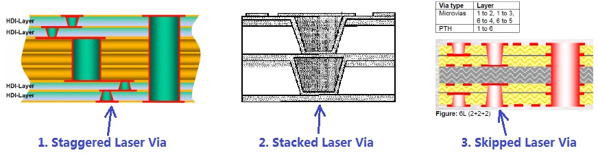
Stacked, staggered and skip-layer laser blind vias; laser vias of 75 µm in mass production, copper-filled blind vias and via-in-pad.
Any-layer (ELIC)
6+C+6 in mass production, 16 layers in samples, and 18-layer samples in 2027.TBC
mSAP fine-line
Line width/spacing in mass production, 25/25 µm in samples; 20 µm planned for the Thailand plant.TBC
High layer count (HLC)
High-layer-count server and networking boards, 3.2 mm thick and up to 450 × 550 mm.TBC
High-speed and high-frequency materials
Materials selected by dissipation factor (Df) grade, including PTFE and hydrocarbon materials, with HVLP copper foil.
Heavy copper
Up to 3 oz inner layers and 4 oz outer layers (samples); 14-layer, 4 oz power boards in production.
Special processes
Back-drilling, stepped and segmented gold fingers, cavities, controlled-depth drilling, POFV, embedded capacitors and resistors, and embedded copper coins.
Process capabilities and 2026–2027 roadmap
Mass-production and sample capabilities are listed separately. 2027 figures are planned values.
Internal review note:Figures are compiled from the 2026 company profiles. Items marked TBC differ between profile versions and must be confirmed by Engineering before launch.
| Item | 2026 mass production | 2026 samples | 2027 mass production | 2027 samples |
|---|---|---|---|---|
| General | ||||
| Maximum layer count TBC | 26 layers | 36 layers | 28 layers | 40 layers |
| Thickness | 0.15–3.2 mm | 0.14–3.2 mm | 0.15–3.2 mm | 0.125–3.2 mm |
| Minimum core thickness | 50 µm | 40 µm | 40 µm | 35 µm |
| Maximum finished board size | 400 × 500 mm | 450 × 550 mm | 450 × 550 mm | 450 × 550 mm |
| Minimum mechanical drill | 0.15 mm | 0.10 mm | 0.15 mm | 0.10 mm |
| Through-hole aspect ratio | 18 : 1 | 20 : 1 | 20 : 1 | 22 : 1 |
| Maximum finished copper (inner/outer) | 3 oz/3 oz | 3 oz/4 oz | 3 oz/4 oz | 4 oz/4 oz |
| Inner-layer line width/spacing (H oz) | 50/50 µm | 40/40 µm | 40/40 µm | 35/35 µm |
| Impedance tolerance | ±10% | ±8% | ±8% | ±7% |
| Bow and twist | ≤ 0.75% | ≤ 0.5% | ≤ 0.75% | ≤ 0.5% |
| HDI and any-layer | ||||
| Any-layer layer count TBC | 14 layers | 16 layers | 16 layers | 18 layers |
| Build-up structure | 6+C+6 | 7+C+7 | 7+C+7 | 8+C+8 |
| Minimum laser via | 75 µm | 65 µm | 75 µm | 65 µm |
| Microvia aspect ratio | 0.75 : 1 | 1 : 1 | 0.8 : 1 | 1 : 1 |
| Copper-fillable via size | 75–125 µm | 65–150 µm | 75–138 µm | 65–150 µm |
| Stacked, staggered, skip vias, via-in-pad | Yes | Yes | Yes | Yes |
| mSAP | ||||
| Maximum layer count | 16 layers | 18 layers | 16 layers | 18 layers |
| Line width/spacing TBC | 30/30 µm | 25/25 µm | 25/25 µm | 20/20 µm |
| BGA pitch TBC | 130–150 µm | 120–130 µm | 120–130 µm | 110 µm |
| Laser via | 60 µm | 60 µm | 60 µm | 60 µm |
| Line width tolerance | ±5 µm | ±4 µm | ±4 µm | ±3 µm |
| Impedance tolerance | ±8% | ±7% | ±7% | ±5% |
| Materials | M7, M8, BT-like, BT | |||
Surface finish
ENIG, ENEPIG, electroplated hard gold and gold fingers, immersion silver, immersion tin, OSP, HASL and lead-free HASL, and flash gold.
Special processes
Back-drilling, stepped gold fingers, segmented gold fingers, cavities, controlled-depth drilling and routing, embedded capacitors, embedded resistors, embedded copper coins, metal-core boards, step PCBs, skip-layer blind vias, resin plugging (POFV) and heavy copper.
Materials
FR4, mid- and high-Tg, lead-free, halogen-free, hydrocarbon, PTFE and low-loss high-speed materials. Material partners include EMC, TUC, ITEQ, Panasonic, Shengyi, Nan Ya, Isola, Nelco and Rogers.
mSAP manufacturing center
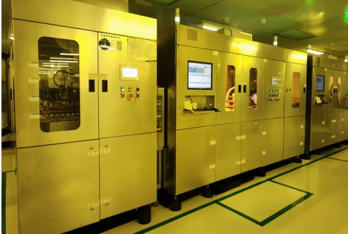
Optical modules and next-generation memory need finer lines and tighter BGA pitch. The Qingyuan plant has a dedicated mSAP workshop where circuits are made on dedicated equipment in a Class 100 cleanroom.
- 30/30 µmMass-production line width/spacing
- ±5 µmLine width tolerance
- 60 µmLaser via
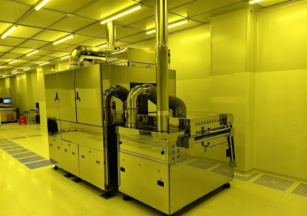
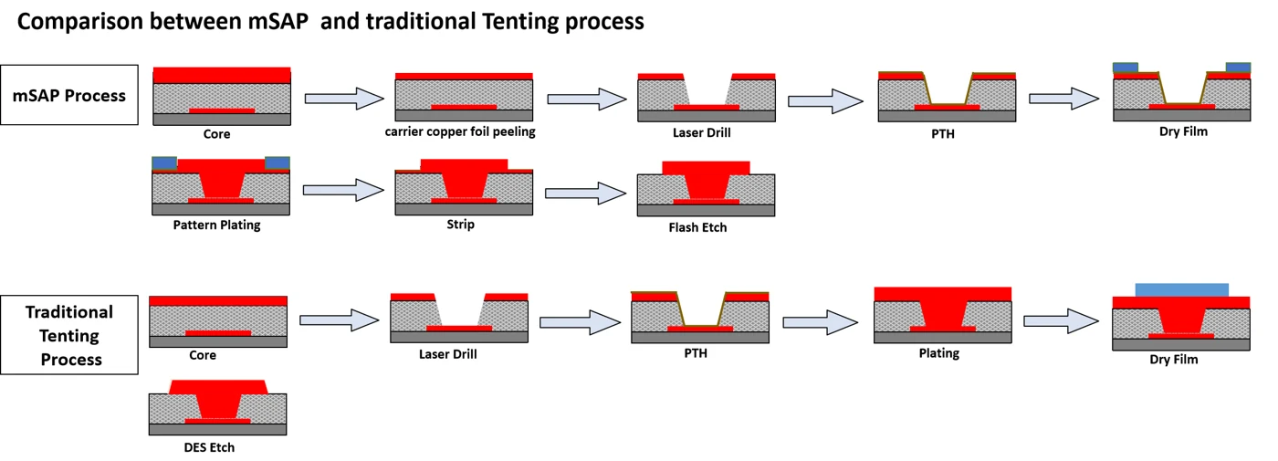
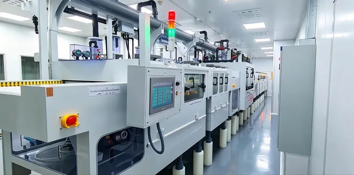
Pattern pretreatment line
Cleans and roughens the copper surface.
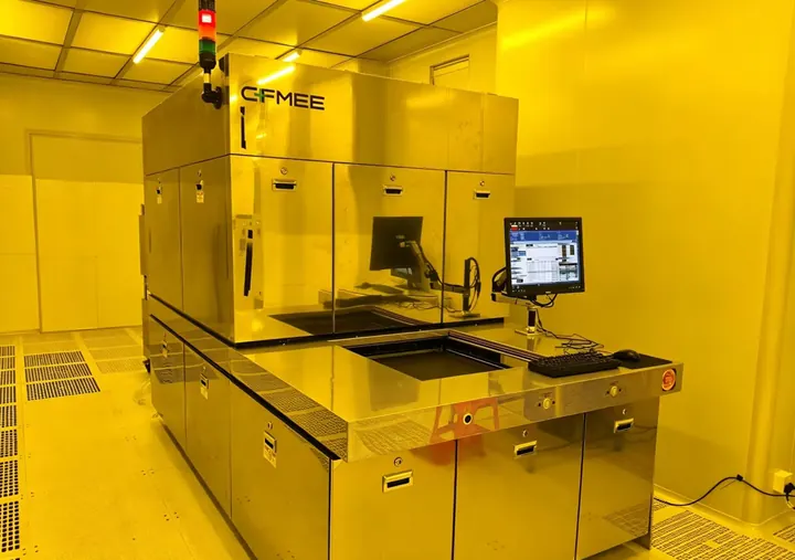
Dedicated LDI exposure
Laser direct imaging in a Class 100 cleanroom.
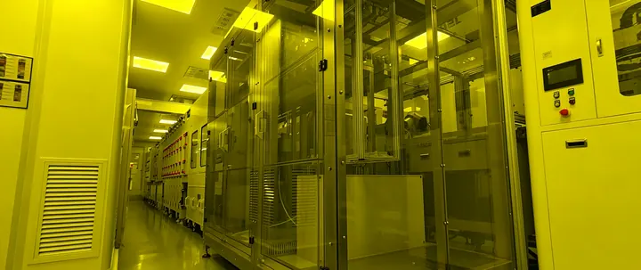
Lamination and dedicated developing line
A dedicated laminator applies dry film, which is developed on a dedicated line after exposure.
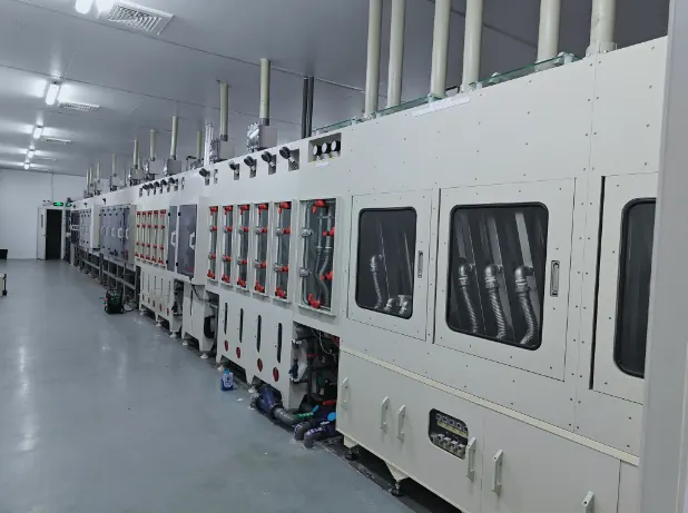
Vertical continuous plating (VCP)
Pattern plating with uniform copper thickness.
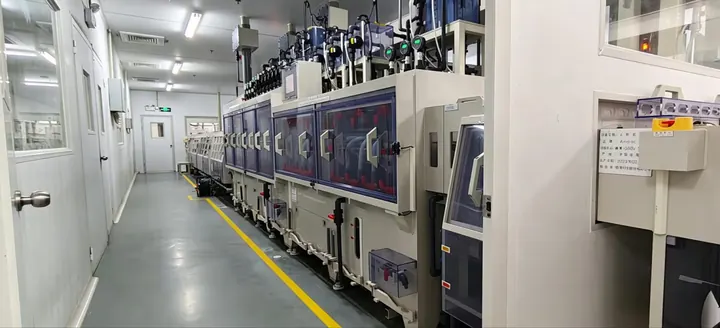
Stripping line
Removes the photoresist.
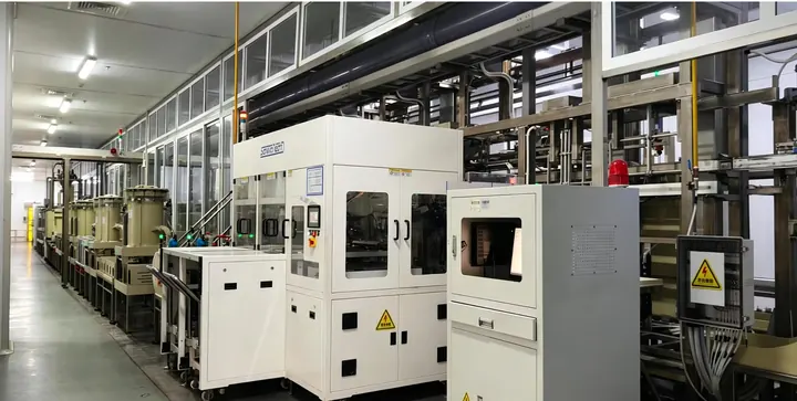
Flash etching line
Removes the seed copper to complete the circuit.
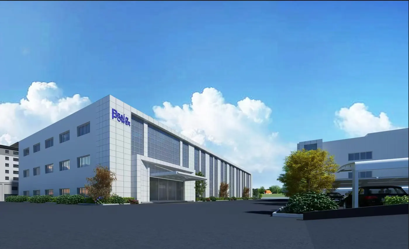
mSAP expansion plan Timing TBC
A 4-story main building (135 × 53 m, 7,155 m² per floor) will be built between the existing plant and dormitories, with 6 mSAP plating lines planned and 2 installed in phase one.
High-Speed Materials & Signal Integrity
From 25G to 224G, each data rate places different demands on material loss and copper roughness. We select materials by data rate and verify them with our own impedance and signal measurement equipment.
Materials by dissipation factor grade
| Grade | Dissipation factor (Df) | Representative materials (partial) |
|---|---|---|
| FR4 | ≥ 0.02 | EM-825, TU-662, IT-180A, S1000-2 |
| M2 | 0.015–0.020 | EM-370Z, TU-862HF, IT-170GRA1, S7045G |
| M4 | 0.010–0.015 | EM-528, TU-863+, M4S, S7439G |
| M6 | 0.006–0.007 | EM-891, TU-883, IT-968, Megtron 6, S6 |
| M7 | 0.005–0.006 | EM-890, TU-933E, IT-988GL, Megtron 7, S6N |
| M7+ | < 0.003 | EM-890K, TU-933+, IT-988GLSE, S8N |
| M8 | < 0.002 | EM-892K, TU-943SN, IT-998G, S9N |
| M8+ | < 0.0015 | EM-892K2, TU-943HR, IT-998GSE, S9N2 |
| M9 | < 0.001 | EM-896K3, IT-999GSE3 |
Per-lane data rate and copper foil
| Per-lane data rate | Copper foil type |
|---|---|
| ≤ 2.5 Gbps | RTF, HTE |
| ≤ 14 Gbps | RTF, HTE |
| 14–28 Gbps | RTF, HTE, VLP |
| 28–56 Gbps | RTF, HVLP, VLP |
| 112 Gbps | RTF, RTF2, HVLP |
| 224 Gbps | RTF, RTF2, HVLP3 |
Impedance control by product type
| Product | Lamination | Mass production | Samples |
|---|---|---|---|
| DAC, MCIO | Core lamination | ±5% | ±3% |
| Prepreg lamination | ±7% | ±5% | |
| AEC, ACC | Core lamination | ±7% | ±6% |
| Prepreg lamination | ±7% | ±7% | |
| AOC | Prepreg lamination | ±10% | ±8% |
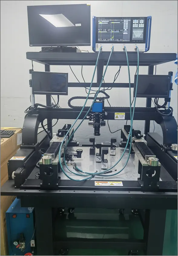
Signal integrity measurement
A signal integrity probe station was installed at the end of 2025. With a network analyzer measuring up to 67 GHz, it measures the insertion loss of channels inside the PCB and is used to validate 224G test boards.
- With the same copper foil and line width, loss from lowest to highest is M8, M7, M6.
- DK02 solder mask ink has lower loss than standard PSR ink.
- HVLP2 copper foil is close to RTF, and both are clearly better than HTE.
- M9-grade EM-896K3 improves insertion loss by about 25% compared with M8-grade EM-892K2.
Impedance control in three stages
- DesignDesign review, impedance simulation, trace compensation, tolerance setting and impedance coupon layout.
- ProductionBatch sampling, cross-sectioning, line width measurement and characteristic impedance testing for high-frequency products.
- ShipmentCross-sectioning and characteristic impedance testing of finished boards, with 100% automated inspection and sorting.
Process & Inspection Equipment
Key equipment and actual measurement data by process stage.
Imaging and circuit formation
LDI exposure, vacuum etchingLDI laser direct imaging
Outer-layer imaging for more uniform line width.
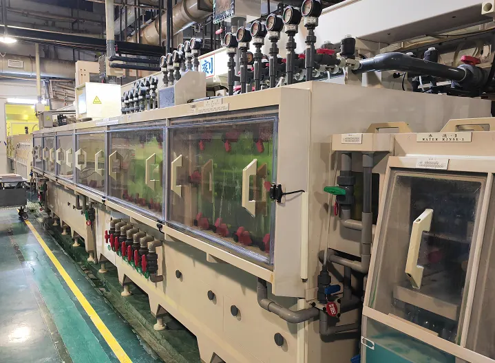
DES vacuum etching line
Forms circuits together with LDI, with an etch factor above 3.
7.2 mil line width, 1.4 mil copper: CPK 2.71, range ≤ 12.5 µm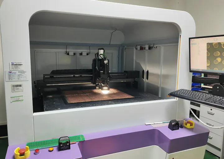
Automatic line width measurement
Nine-point measurement, with full first-article inspection and sampling every 2 production lots.
Line width tolerance ±0.25 milPlating and surface finish
VCP, ENEPIG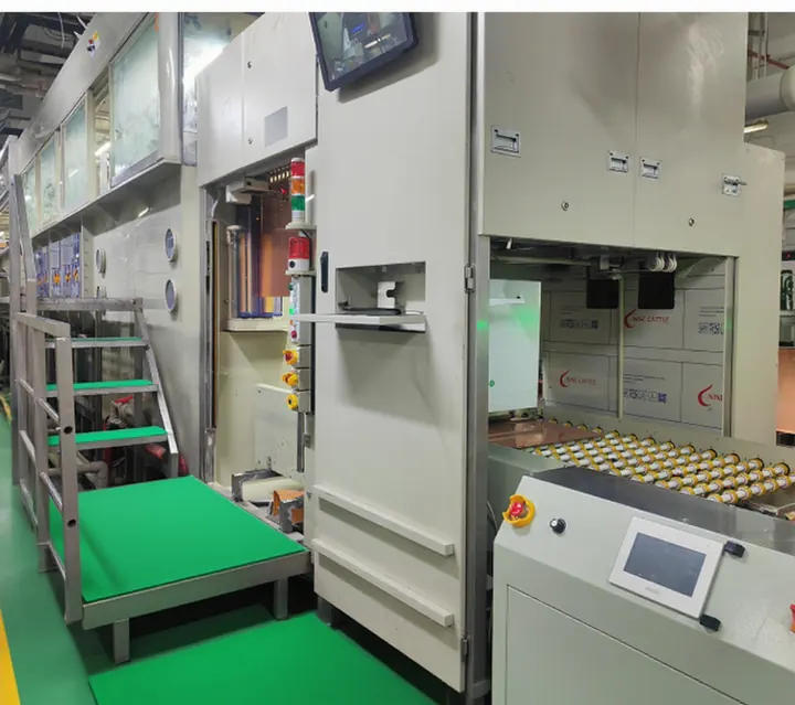
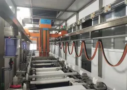
VCP vertical continuous plating
Dedicated plating for mass production, with copper thickness variation held to 2.5–5 µm.
C side CPK 1.92 · S side CPK 1.99 · range ≤ 5 µm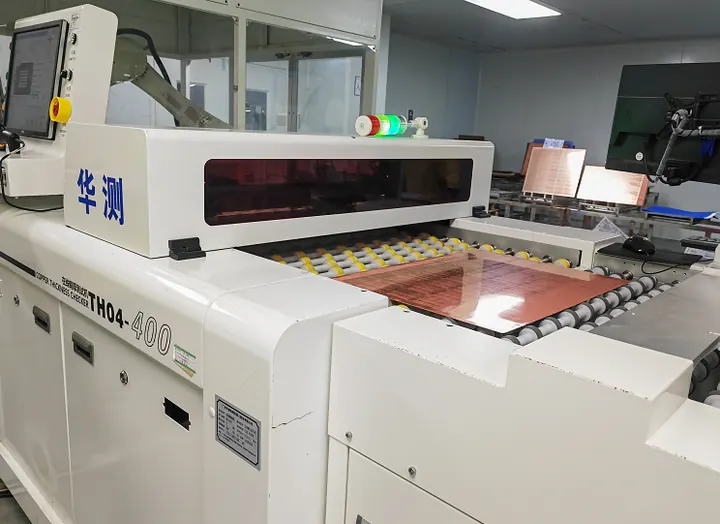
Automatic copper thickness measurement
100% inspection of plated copper thickness, with automatic sorting when the range exceeds 5 µm.
Dedicated ENEPIG line
Dual chemistry system with in-line pH and conductivity monitoring and a bath filtration system.
Wire pull ≥ 3 gf · ball shear ≥ 35 gfRouting and dimensions
CCD alignment, gold finger beveling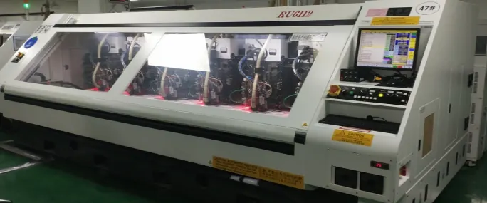
CCD CNC routing
Routes board outlines using CCD vision alignment.
Circuit-to-edge tolerance ±0.05 mm · CPK > 1.67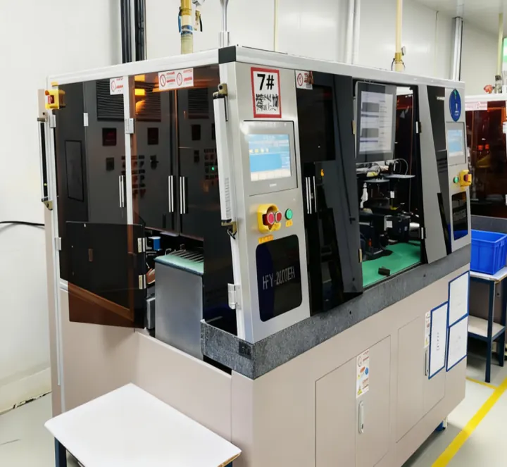
Gold finger bevel
CCD cameras at both tool entry and exit follow the actual contour.
Angle 45 ± 5° · CPK 2.43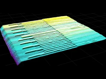
3D bevel inspection
Dual-camera 3D imaging with real-time results, defect location marking and fully automatic loading and unloading.
X/Y repeatability ±5 µm · overall ±1.0 µmImpedance and signal measurement
100% impedance testing, 67 GHz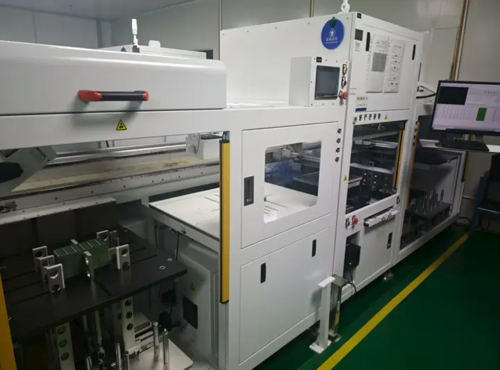
Fully automatic impedance testing
100% testing of finished boards, automatically sorting pass and fail boards.
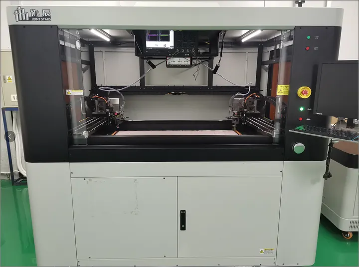
Flying-probe impedance testing
Measures actual boards, with frequency parameters set to customer requirements, down to 11.2 ps.
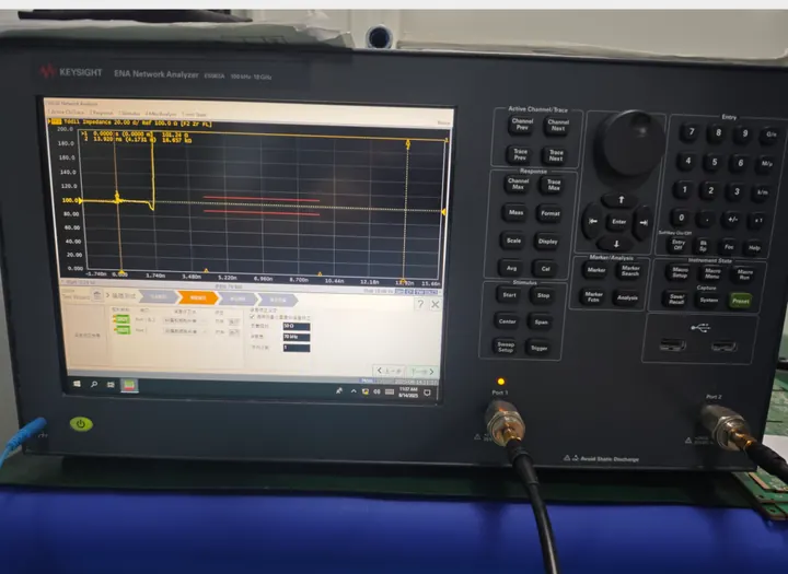
First-article impedance control
First-article tolerance tightened to 80% of the specification.
Plating and microanalysis
X-ray thickness gauge, 3D measuring microscope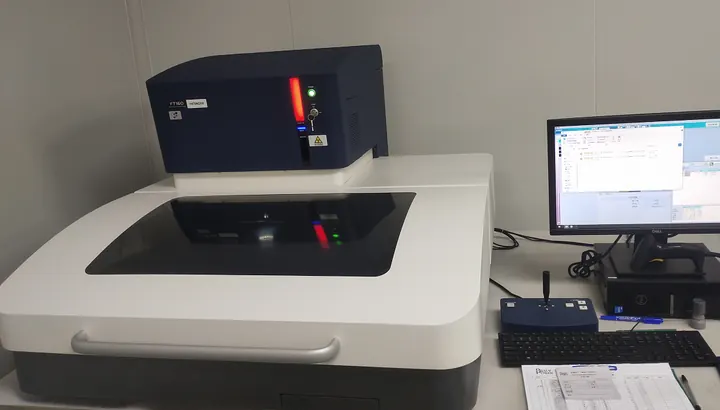
Polycapillary X-ray thickness gauge
Hitachi FT160, analyzing all 4 layers of ENEPIG plating.
Minimum pad 30 µm · error < 5%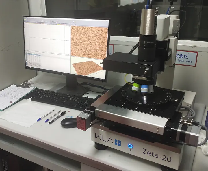
3D laser measuring microscope
KLA Zeta-20, measuring surface roughness, blind via and plugged via profiles, back-drill depth and bevel angle.
Resolution 0.1 nm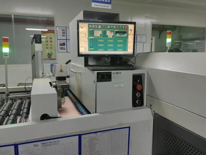
Laser board thickness measurement
Nine-point measurement after lamination with 100% inspection, data uploaded to MES in real time.
Reliability and chemistry labs
17+ measurements and tests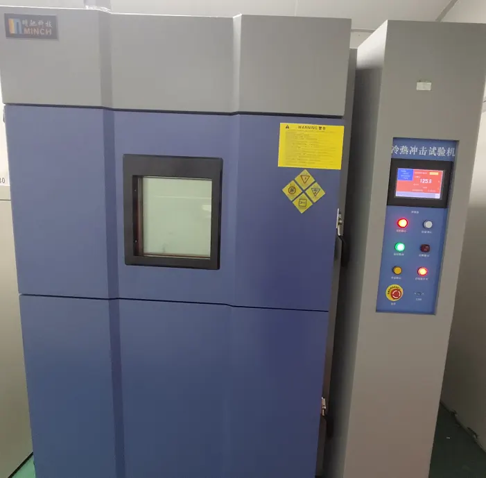
Thermal cycling (TCT)
Thermal cycling reliability testing.
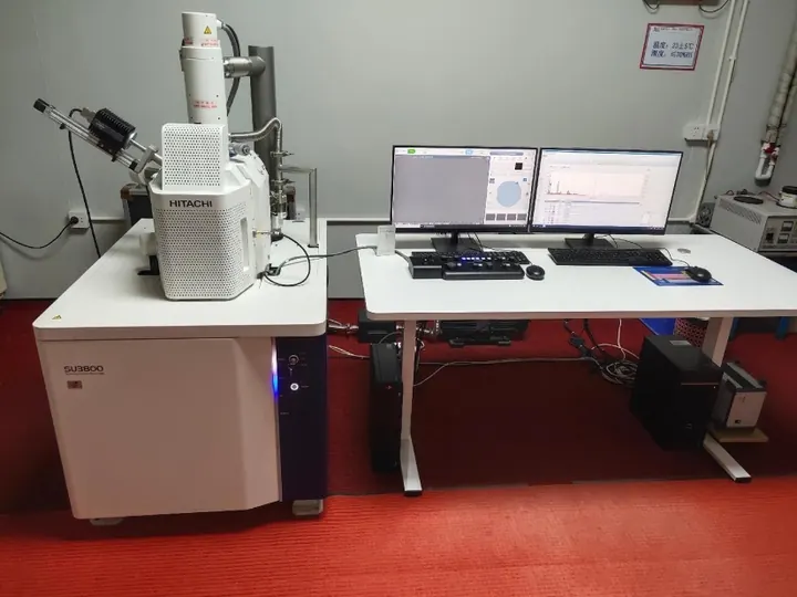
SEM and EDS
Microstructure observation and composition analysis.
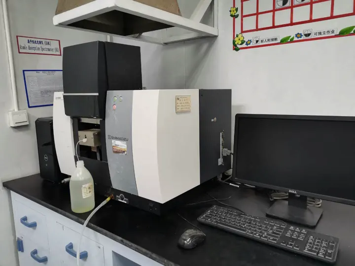
Atomic absorption spectrometer
Analysis of metal ion concentration in baths.
- Reflow oven, temperature and humidity chamberHeat resistance and temperature-humidity testing
- SIR and CAF testingSurface insulation resistance, conductive anodic filament
- Salt spray tester, tensile testerCorrosion resistance, peel strength
- Differential scanning calorimetry (DSC)Tg measurement
- RoHS analyzerHazardous substance screening
- Ion chromatographIonic contamination measurement
- Automatic potentiometric titratorBath concentration, data uploaded to MES in real time
- UV spectrophotometer, CVS analysisPlating additive analysis
- COD, conductivity and pH measurementWastewater and bath monitoring
- Hull cell testingPlating solution evaluation
- Static resistance and wrist strap testerESD control
- Drill quality analyzer, hole position inspectionDrill quality and hole position accuracy
Quality systems
Our QA and QC team of 36 runs a chemistry lab and a physics lab. Data from every station comes from ERP and MES and supports management decisions.
- Incoming inspection (IQC)Analysis of raw materials and chemicals.
- In-process control (IPQA)First articles for new part numbers, process audits, sampling, line stops and control of nonconforming products.
- 100% electrical and visual inspectionFunctional testing and visual inspection, with AI-assisted AVI.
- Outgoing inspection (FQA/OQC)Reliability testing and outgoing quality inspection.
- Customer feedbackIncoming inspection results and quality performance at the customer feed into improvement.
Complaint response times
- Containment actions
- Within 24 hours
- 8D report (appearance, packaging)
- 5 working days
- 8D report (functional)
- 7 working days
Where a customer specifies other deadlines, we meet the customer’s requirement.
MES and SPC
Over 90% of the equipment at the Qingyuan plant is connected to MES. Work orders are controlled by barcode scanning and lock automatically if they run overtime or on equipment other than specified. MES calculates SPC automatically to CPK ≥ 1.33 across 7 product parameters and 22 chemistries, and abnormalities trigger instant email alerts.
AI inspection
AI review is fully deployed on solder mask AVI and final FQC AVI and partly on inner- and outer-layer AOI, cutting false calls by more than 80%. The Thailand plant will deploy it fully, targeting a reduction of more than 90%.
International management system certifications
The following certificates are held by Brain Power (Qing Yuan) Co., Ltd.
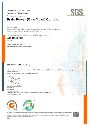
Automotive quality management · CN13/31554
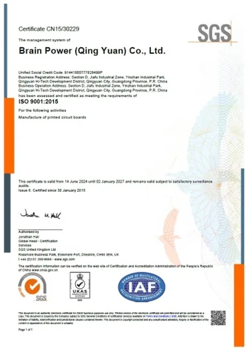
Quality management · CN15/30229
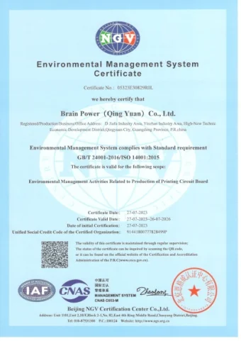
Environmental management · 05323E30829R0L
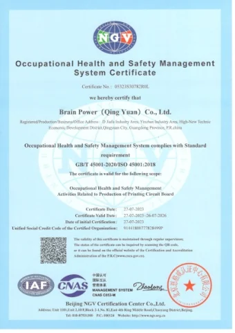
Occupational health and safety · 05323S30782R0L
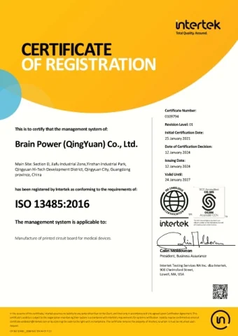
Medical device quality management · 0109794
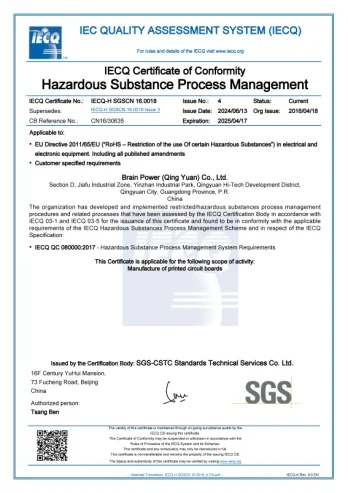
Hazardous substance management · CN16/30635
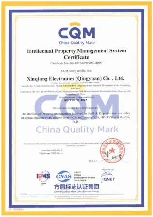
Intellectual property management · 00224IPMS0225R0M
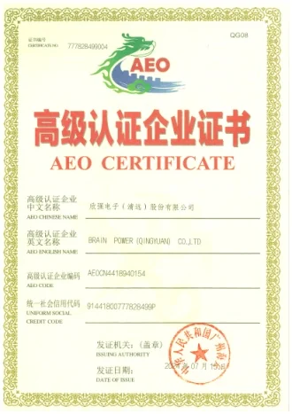
Customs certification · 777828499004
Need the full capability table or stack-up advice?
Share your application and specifications, and our engineering team can help evaluate materials, stack-up and impedance design.